Incheon National University Department of Materials Science and Engineering Professor Hanboram Lee’s team ‘Atomic Layer Deposition Equipment and Atomic Layer Deposition Process’ technology transfer
- 글번호
- 413357
- 작성일
- 2025-09-30
- 수정일
- 2025-09-30
- 작성자
- 홍보과 (032-835-9490)
- 조회수
- 245
.png)
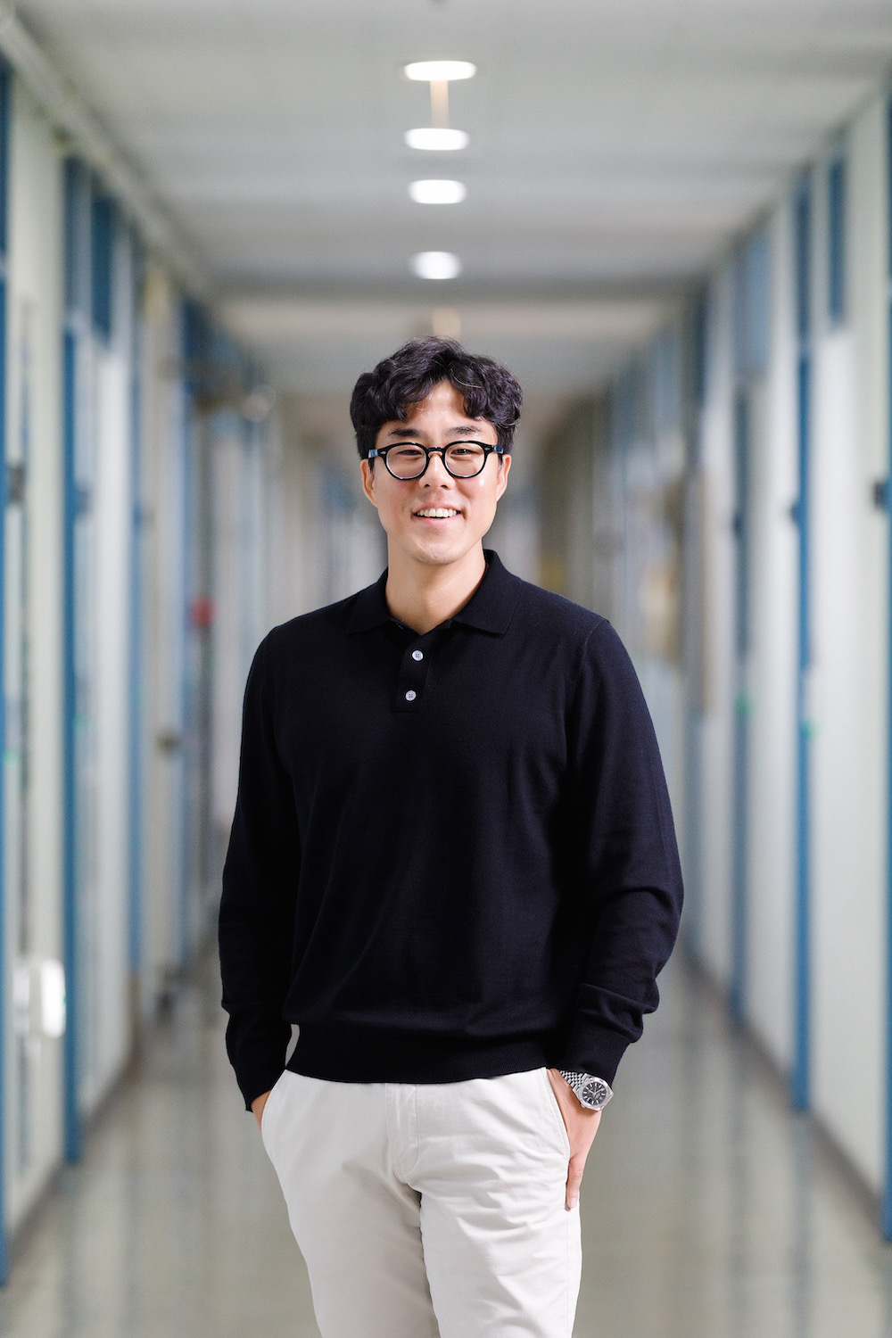
Left) Professor Hanboram Lee, Incheon National University / Right) Gyeongmin Min (Integrated M.S.–Ph.D. program)
- Technology transfer of a new semiconductor metal process for faster AI computation
Incheon National University and CN1 Co., Ltd. have signed a technology transfer agreement, accelerating the commercialization of advanced semiconductor process technology.
This technology is a method for forming high-quality metal conductors during semiconductor chip manufacturing and is evaluated as a substitute for metals such as copper that have been used so far. Once applied to semiconductor chip production, it is expected to be highly effective in driving chips at extremely fast speeds, significantly impacting AI computation speed and performance.
The Incheon National University Industry-Academic Cooperation Foundation (Director: Donggu Kang) announced on the 24th that Professor Hanboram Lee’s research team from the Department of Materials Science and Engineering signed a technology transfer agreement with CN1 Co., Ltd. (CEO: Jaehak Jung), a specialized semiconductor and display equipment company.
The transferred technology concerns “Atomic Layer Deposition Equipment and Atomic Layer Deposition Process” and is valued at 800 million KRW. Notably, it has great significance for overcoming the previous limitations in atomic layer deposition of ruthenium (Ru), a next-generation semiconductor metal material, where the use of oxidizers or plasma had been inevitable.
The research team enabled the generation of atomic hydrogen during the process, allowing the formation of high-purity thin films. This breakthrough overcame the need for conventional oxidizers and resolved the issue of interface oxide formation. In addition, the team presented solutions to improve step coverage problems frequently occurring in plasma processes, while also achieving stable deposition under low-temperature conditions, reducing the risk of device damage. This technology is regarded as an important advancement that can contribute to securing competitiveness in next-generation semiconductor metallization processes, maintaining stable electrical properties of semiconductor devices while supporting accelerated miniaturization.
Since its establishment in 2008, CN1 Co., Ltd. has focused on the R&D market in the pre-mass-production stage of semiconductors, supplying equipment to major domestic companies and research institutes such as Samsung Electronics. Through this technology transfer, the company plans to strengthen its advanced ALD equipment development capabilities and further solidify its position as a provider of next-generation semiconductor process solutions.
Director Donggu Kang of the Incheon National University Industry-Academic Cooperation Foundation stated, “This technology transfer is a representative case of how the university’s research achievements can solve industrial challenges and lead to commercialization,” and added, “We will continue to expand cooperation with outstanding domestic companies like CN1 to contribute to enhancing the global competitiveness of Korea’s semiconductor equipment industry.”